An eight-transistor (8T) SRAM cell is proposed to improve variability tolerance and low-voltage operation in high-speed SRAM caches. No need for secondary or dynamic power supplies. The proposed 8T solution is demonstrated in a high-performance 32 kb subarray designed in 65 nm PD-SOI (Partially-Depleted Silicon-On-Insulator) CMOS that operates at 5.3 GHz at 1.2 V and 295 MHz at 0.41 V.
An 8T-SRAM for Variability Tolerance and Low-Voltage Operation in High-Performance Caches
Leland Chang et. al. — IBM T. J. Watson Research Center
Journal of Solid-State Circuits (JSSC) · 2008
Principle of SRAM cell transistor sizing
At the cell level, transistor strength ratios must be chosen such that cell static noise margin and write margin are both maintained, which presents conflicting constraints on the cell transistor strengths.
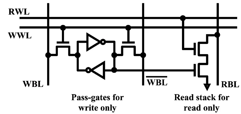
For cell stability during a read, it is desirable to strengthen the storage inverters and weaken the pass-gates. The opposite is desired for cell writability: a weak storage inverter and strong pass-gates. This delicate balance of transistor strength ratios can be severely impacted by device variation, which dramatically degrades stability and write margins, especially in scaled technologies. Low supply voltages further exacerbate the problem as threshold voltage variation consumes a larger fraction of these voltage margins.
Design Notes
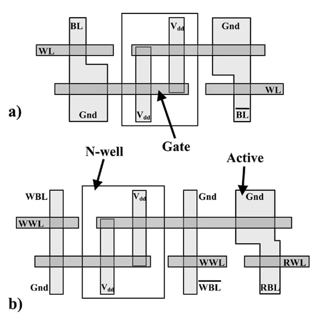
For the high-performance applications targeted in this work, the fabricated 8T cell size in 65 nm hardware is 0.9μm2. No additional process steps (implant masks, gate oxides, etc.) on top of a standard flow were used to build this cell.
To improve cell write margins and reduce cell area, it is desirable to minimize the width of the pull-down nFET. While this increases variation, a write margin improvement will generally be observed. Further write margin enhancement can be achieved by strengthening the pass-gate devices — either by lowering VT , reducing gate length, increasing device width, or expanding WWL voltage swing. Since these techniques do not affect stability, 8T cells can simultaneously improve both stability and writability yields. These techniques may, however, come at the cost of cell leakage.
Depending on the balance between gate and subthreshold leakage current levels, migration from a 6T cell to an 8T cell at the same supply voltage may increase cell leakage somewhat as pass-gate leakage and the two additional read stack transistors offset the minimum-width, high-VT pull-down nFETs and pull-up pFETs. On the other hand, this may be an issue since voltage scaling is enabled by 8T-SRAM, which reduces leakage currents. It should also be noted that due to asymmetry in the cell read stack, cell leakage is data-dependent.
Read performance in an 8T cell is determined by the strength of the two-transistor read stack. Due to layout restrictions, the top read transistor is generally of smaller width, and thus likely limits read current. Cell write performance will largely be determined by the pass-gate device strength, but may also be affected somewhat by asymmetric loading of the storage nodes due to the read transistor; however, any slowdown will be mitigated by minimization of the pull-down nFET size. Without stability or write margin concerns, 8T cell performance—like regular logic—is limited only by normal power, performance, and area tradeoffs.
Cell Disturbs due to unselected columns: While the 8T cell removes read stability concerns, cell disturbs can also occur in unselected columns during a write event. In this case, the write word line may be turned on while the write bit lines (held high) are relied upon to ensure cell stability—a situation identical to a read disturb in a 6T cell. While it is possible to optimize an 8T cell to withstand such write disturbs, any cell stability advantage would be lost. Instead, this issue must be addressed by the array organization by entirely prohibiting the column select condition in an 8T array.